
 Home
Home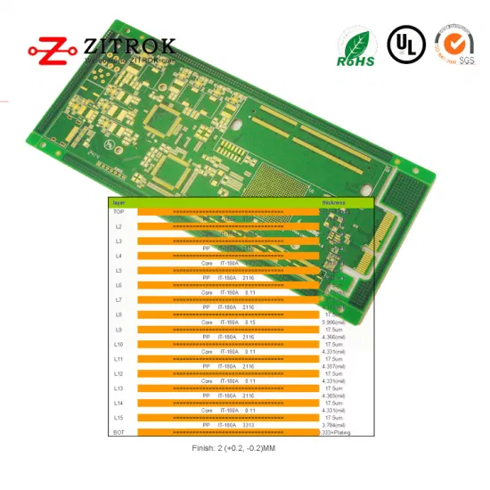

Fast Turn Rigid Flex Mini PCB Layout Services Custom Printed Circuit Board in Computer
Finest Group was established in April 2003, focusing on PCB board manufacturing, SMT processing, and components support
Basic Info.
| Model NO. | custom printed circuit board |
| Processing Technology | Electrolytic Foil |
| Base Material | Copper |
| Insulation Materials | Organic Resin |
| Brand | Finestpcb |
| Board Thickness | 1.6 ±0.1mm |
| Minimum Hole | Minimum |
| Copper Thickness | 0.5-5oz |
| Minimum Line | 3/3mil |
| Product Name | OEM PCB PCBA Board Assembly |
| Minimum Width | 3/3mil |
| Min BGA Ball Pitch | 0.4mm |
| HASL\OSP\Immersion Gold | Fr4/Rogers/Aluminum/High Tg |
| Surface Finishing | HASL\OSP\Immersion Gold |
| Solder Mask Color | Blue.Green.Red.Black.White |
| Layer | 1-40layers |
| Service | One-Step PCB Service |
| Transport Package | Vacuum Package for Bare PCB and ESD Package |
| Specification | customized |
| Trademark | finest |
| Origin | China |
| HS Code | 8534001000 |
| Production Capacity | 30000 Pieces |
Product Description
Finest Group was established in April 2003, focusing on PCB board manufacturing, SMT processing, and components support services.
FINEST PCB Assemble Ltd is a subsidiary of FINEST Group. It was established on April 2019, specializing in EMS Processing, SMT quick-turn prototype, and small batch production. Finest PCBA team with the ability to select materials, make samples and small batch production, and donging testing services. We always improve research and development efficiency, aiming at providing fast service to satisfy customers' different demands for PCB assembly.
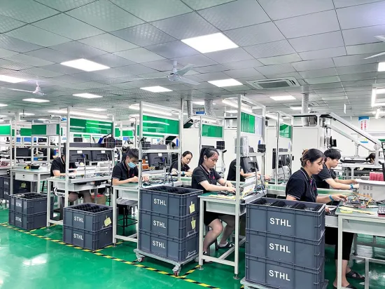
The SMT factory is located in Fuyong, Shenzhen, with a plant area of 2500m'and8 SMT production lines. Equipped with new imported Hanwha 471, 481, 482, automatic solder paste printers, ten-temperature zone reflow soldering, wave soldering, and other high-tech equipment. Besides, factories also have advanced. AOI, X-RAY, SPI, intelligent first article tester, BGA rework station, etc. Factories develop the newest technology and invest in the best equipment to improve our production ability and focus on R&D, prototyping, small batch SMT assembly, and other services.
We have a series of resistors and capacitors and common inductances, magnetic beads.
connectors, crystal oscillators, and diode triodes, and provide full BOM component supporting services for research and development.
FINEST PCB factory is located in Humen, Dongguan. We are a high-tech enterprise, with first-class processing equipment, that focuses on single-side, double-sided, and multi-layer PCB manufacturing.
One-stop PCB and PCB assembly, components, SMT & EMS services, with fast delivery time, good quality, and best communication support.
Why choose Finest PCB Assembly? 1. More than 19 years experience of in electronic manufacturing services for PCB making. 2. One-stop service | PCB Manufacturing | Components sourcing and PCB assembly one-stop PCBA service to help you easily achieve your electronic products. 3. More than 1000 customers working with us for telecom, IOT, RF, smart control, security, medical, industrial, automotive, 3G / 4G / 5G products.4. Reasonable and stable price: have established a strong global electronics components supply chain that helps us getreasonable and stable price 5. Quality assurance: more than 15 years of experience in the engineering team and quality control team to ensureall products come out under control.6. Professional replace-solution: help customers source professional replace-solution to achieve faster, lower cost with high-quality components purchasing agent service.
| PCBA Technical Capability | |
| 1. Assembly Type:: | FR4, FPC, Rigid-flex PCB, Metal base PCB. |
| 2. Assembly Specification: | Min size L50*W50mm; Max size: L510*460mm |
| 3. Assembly thickness: | Min thickness: 0.2mm; Max thickness: 3.0mm |
| 4. Components Specification | |
| Components DIP: | 01005Chip/0.35 Pitch BGA |
| Minimum device accuracy: | +/-0.04mm |
| Minimum footprint distance: | 0.3mm |
| 5. File format: | BOM list; PCB Gerber file: |
| 6. Test | |
| IQC: | Incoming inspection |
| IPQC: | Production inspection; first ICR test |
| Visual QC: | Regularly quality inspection |
| SPI test : | Automatic solder paste optical inspection |
| AOI: | SMD component welding detection, components shortage & component polarity detection |
| X-Ravd: | BGA test; QFN and other precision devices hidden PAD device inspection |
| Function test: | Test function and performance according to the customer's test procedures and steps |
| 7. Reworking: | BGA rework equipment |
| 8. Delivery Time | |
| Normal delivery time: | 24 hours( fastest 12 hours quick-turn) |
| Small production: | 72 hours( fastest 24 hours quick-turn) |
| Medium production: | 5 working days. |
| 9. Capacity: | SMT assembly 5 million points/day; plug-in & welding 300,000 points/day; 50-100 items/day |
| 10. Components Service | |
| A full set of substitute materials: | Have experience in component procurement sourcing, and management systems, and provide cost-effective services for OEM projects |
| Only SMT: | Do SMT and backhand welding according to components PCB boards provided by customers. |
| Components purchasing: | Customers provide core components, and we provide component sourcing services. |
| PCB Specification: | |||||
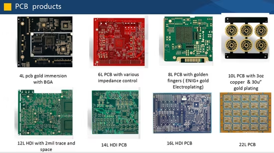
| PCB layers: | 1-24layers | ||||
| PCB materials: | CEM1, CEM3, Rogers, FR-4, High Tg FR-4, Aluminum Base, Halogen Free | ||||
| PCB max. board size: | 620*1100mm (Custom) | ||||
| PCB certificate: | RoHS Directive-Compliant | ||||
| PCB Thickness: | 1.6 ±0.1mm | ||||
| Layer Copper Thickness: | 0.5-5oz | ||||
| Inner Layer Copper Thickness: | 0.5-4oz | ||||
| PCB max. board thickness: | 6.0mm | ||||
| Minimum Hole Size: | 0.20mm | ||||
| Minimum Line Width/Space: | 3/3mil | ||||
| Min. S/M Pitch: | 0.1mm(4mil) | ||||
| Plate Thickness and Aperture Ratio : | 30:1 | ||||
| Minimum Hole Copper: | 20µm | ||||
| Hole Dia. Tolerance(PTH): | ±0.075mm(3mil) | ||||
| Hole dia. Tolerance(NPTH): | ±0.05mm (2mil) | ||||
| Hole Position Deviation: | ±0.05mm (2mil) | ||||
| Outline Tolerance: | ±0.05mm (2mil) | ||||
| PCB solder mask: | Black, white, yellow | ||||
| PCB surface finished: | HASL Lead-free, Immersion ENIG, Chem Tin, Flash Gold, OSP, Gold finger, Peelable, Immersion Silver | ||||
| Legend: | White | ||||
| E-test: | 100% AOI, X-ray, Flying probe test. | ||||
| Outline: | Rout and Score/V-cut | ||||
| Inspection Standard: | IPC-A-610CCLASSII | ||||
| Certificates: | UL (E503048),ISO9001/ISO14001/IATF16949 | ||||
| Outgoing Reports: | Final Inspection, E-test, Solderability Test, Micro Section, and More | ||||
FAQ1. who are we?We are based in Guangdong, China, and start from 2019, sell to Domestic Market(50.00%), North America(15.00%), SouthAmerica(12.00%),Northern Europe(12.00%),Western Europe(5.00%),Southeast Asia(2.00%),Mid East(2.00%),Eastern Europe(2.00%). Thereare a total of about 301-500 people in our office.2. how can we guarantee quality?Always a pre-production sample before mass production;Always final Inspection before shipment;3. what can you buy from us?PCBA, PCB Assembly, PCBA Board, LED PCBA, Electronic PCBA4. why should you buy from us not from other suppliers?*A 18-year one-stop solution provider *Strong R&D group with 30 engineers *Monthly output:45000 sqm of PCBs and PCBAs*4500-square-meter factory *Eight SMT production-line *Automatic SMT, Reflow machine, AOI&x-RAY *Fast response, reply within 24hrs5. what services can we provide?Accepted Delivery Terms: FOB, CIF, EXW, Express Delivery;Accepted Payment Currency: USD, EUR, GBP;Accepted Payment Type: T/T, L/C, MoneyGram, Western Union;Language Spoken: English, French
Send to us