
 Home
Home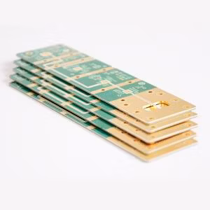


Immersion Gold Multilayer PCB, HDI Printed Circuit Board with Blind and Buried Vias
Immersion Gold Multilayer PCB, HDI Printed Circuit Board with Blind and Buried Vias 1. Single, Double side & Multi-layer
Basic Info.
| Model NO. | PCB-A1 |
| Processing Technology | Electrolytic Foil |
| Base Material | Kingboard |
| Insulation Materials | Epoxy Resin |
| Brand | Abis |
| Layers | 1-20layers |
| Hard Gold Thickness | 1-50u′′ |
| Certification | UL,ISO9001&ISO14001,SGS,RoHS,IATF16949 |
| Copper Thickness | 0.5-8oz |
| Enig Thickness | 1-3u′′ |
| Board Thickness | 0.2-6mm |
| Holes Specification | Buried/Blind Vias, Via in Pads, Counter Sink Hole |
| Transport Package | Vacuum Packing |
| Specification | Custom |
| Trademark | Abis Circuits |
| Origin | Shenzhen, China |
| HS Code | 85340010 |
| Production Capacity | 720, 000 M2/Year |
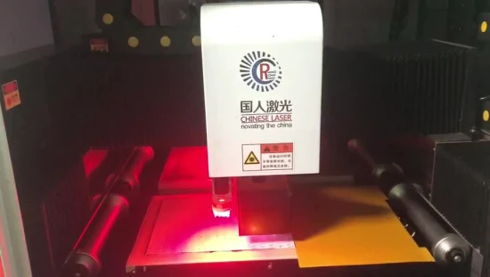
Product Description
Immersion Gold Multilayer PCB, HDI Printed Circuit Board with Blind and Buried Vias
1. Single, Double side & Multi-layer PCB.
2. Buried/Blind Vias, Via in Pad, Counter Sink Hole, Screw Hole(Counterbore), Press-fit, Half Hole.
3. HASL lead-free, Immersion Gold/ Silver/Tin, OSP, gold plating/finger, Peelable mask, Carbon ink.
4. Printed Circuit Boards adhere to IPC Class 2 & 3 international PCB standards.
5. Quantities range from prototype to medium&big batch production.
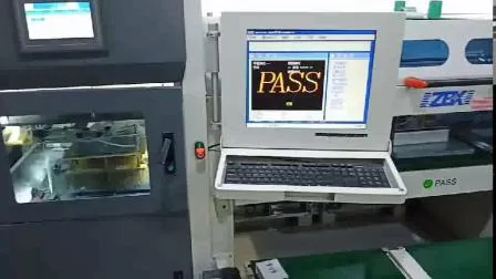
6.100% E-Test.
Technical & Capability
| Item | Production Capacity |
| Layer Counts | 1-20 layers |
| Material | FR-4,Cu base,High TG FR-4,PTFE,Rogers,TEFLON etc. |
| Board thickness | 0.20mm-8.00mm |
| Maximum Size | 600mmX1200mm |
| Board Outline Tolerance | +0.10mm |
| Thickness Tolerance(t≥0.8mm) | ±8% |
| Thickness Tolerance(t<0.8mm) | ±10% |
| Insulation Layer Thickness | 0.075mm--5.00mm |
| Minimum Line | 0.075mm |
| Minimum Space | 0.075mm |
| Out Layer Copper Thickness | 18um--350um |
| Inner Layer Copper Thickness | 17um--175um |
| Drilling Hole(Mechanical) | 0.15mm--6.35mm |
| Finish Hole(Mechanical) | 0.10mm-6.30mm |
| Diameter Tolerance(Mechanical) | 0.05mm |
| Registration(Mechanical) | 0.075mm |
| Aspect Ratio | 16:1 |
| Solder Mask Type | LPI |
| SMT Mini.Solder Mask Width | 0.075mm |
| Mini. Solder Mask Clearance | 0.05mm |
| Plug Hole Diameter | 0.25mm--0.60mm |
| Impedance control Tolerance | ±10% |
| Surface finish/treatment | HASL, ENIG, Chem, Tin, Flash Gold, OSP, Gold Finger |
| Production capacity of hot-sale products | |
| Double Side/Multilayer PCB Workshop | Aluminum PCB Workshop |
| Technical Capability | Technical Capability |
| Raw materials: CEM-1, CEM-3, FR-4(High TG), Rogers, TELFON | Raw materials: Aluminum base, Copper base |
| Layer: 1 layer to 20 Layers | Layer: 1 layer and 2 Layers |
| Min.line width/space: 3mil/3mil(0.075mm/0.075mm) | Min.line width/space: 4mil/4mil(0.1mm/0.1mm) |
| Min.Hole size: 0.1mm(dirilling hole) | Min.Hole Size: 12mil(0.3mm) |
| Max. Board size: 1200mm* 600mm | Max.Board size: 1200mm* 560mm(47in* 22in) |
| Finished board thickness: 0.2mm- 6.0mm | Finished board thickness: 0.3~ 5mm |
| Copper foil thickness: 18um~280um(0.5oz~8oz) | Copper foil thickness: 35um~210um(1oz~6oz) |
| NPTH Hole Tolerance: +/-0.075mm, PTH hole Tolerance: +/-0.05mm | Hole position tolerance: +/-0.05mm |
| Outline Tolerance: +/-0.13mm | Routing outline tolerance: +/ 0.15mm; punching outline tolerance:+/ 0.1mm |
| Surface finished: Lead-free HASL, immersion gold(ENIG), immersion silver, OSP, gold plating, gold finger, Carbon INK. | Surface finished: Lead-free HASL, immersion gold(ENIG), immersion silver, OSP, etc |
| Impedance control tolerance: +/-10% | Remain thickness tolerance: +/-0.1mm |
| Production capability: 50,000 s.q.m/month | MC PCB Production capability: 10,000 s.q.m/month |
Q/T Lead Time
| Category | Quickest Lead Time | Normal Lead Time |
| Double-sided | 24hrs | 120hrs |
| 4 Layers | 48hrs | 172hrs |
| 6 Layers | 72hrs | 192hrs |
| 8 Layers | 96hrs | 212hrs |
| 10 Layers | 120hrs | 268hrs |
| 12 Layers | 120hrs | 280hrs |
| 14 Layers | 144hrs | 292hrs |
| 16-20 Layers | Depends on the specific requirements | |
| Above 20 Layers | Depends on the specific requirements | |
Quality ControlPre-Sale and After-Sale Service 1 Hour quotation2 hours of complaint feedback7*24 hour technical support7*24 order service7*24 hour delivery7*24 production runCompany Profile
Abis Circuits Co., Ltd, is a professional PCB manufacturer which was established in Oct 2006. Focus on double side, Multilayer, and HDI PCB mass production.We have two factories together. The factory in Shenzhen is specialized in small and middle-volume orders. Another in Jiangxi province is for big volume and HDI.
Factory:
Operation plant space: (I) 10000 Square meters
(II) 60000 Square meters
Employees: (I) 300 Man Powers
(II) 900 Man Powers
Eng. Technical: (I) 20 QA QC Engineers
(II) 60 QA, QC Engineers
Certification Standards
Company Show
FAQQ1:When can I get the quotation?
A: We usually quote 1 hour after we get your inquiry. If you are very urgent, please call us or tell us in your email.Q2:Can you provide free samples for me?
A: Free samples depend on your order quantity.Q3:I am a small wholesaler, do you accept small orders?
A: It's no problem. If you're a small wholesaler, we would like to grow up with you together.Q4:How many days will the sample be finished? And how about mass production?
A: Generally 2-3 days for sample making. The lead time of mass production will depend on the order quantity and the season you place the order.Q5:If I order a big quantity, what's the good price?
A: Please send the details inquiry to us, such as the Item Number, Quantity for each item, Quality request, Logo, Payment Terms, Transport method, Discharge place, etc. We will make an accurate quotation for you as soon as possible.Q6: How can we know the processing of PCB orders?
A: Each Customer will have a sale to contact with you. Our working hours: AM 9:00-PM 19:00(Beijing Time) from Monday to Friday. We will reply to your email as soon as quickly during our working time. And you also could contact our sales by cellphone if urgent.Q7:Can I have samples to test?
A: Yes, we are pleased to supply module samples to test and check the quality, mixed sample order is available. Please note buyer should pay for the shipping cost.Q8:Can you design PCB and make files for us?
A: yes, We have a professional drawing engineers' team that you can trust.Q9:If all PCB, PCBAs will be tested before delivery if we provide the function testing method?
A: Yes, we ensure that each piece of PCB, and PCBA will be tested before shipment, and we ensure the goods we sent with good qualityQ10:What is the shipping method?
A: We suggest you use DHL, UPS, FedEx, and TNT forwarder.Q11:How about the payment terms?
A: By T/T, Paypal, Western Union, etc.Why choose us?·With ABIS, customers significantly and effectively reduce their global procurement costs. Behind each service provided by ABIS, is hidden a cost-saving for customers.. We have two shops together, one is for prototype, quick turn, and small volume making. The other is for mass production also for HDI board, with highly skilled professional employees, for high-quality products with competitive price and on-time delivery.. We provide very professional sales, technical and logistic support, on a worldwide basis hours of complaint feedback.
Please keep us informed of any interest!ABIS cares about every your order even 1 piece!
Send to us