
 Home
Home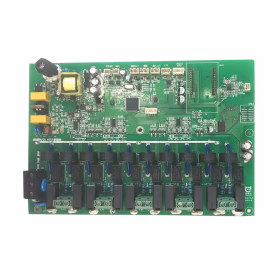

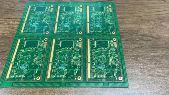
Multilayer 1
Product Specifications: Layers: 6LMaterial: Fr-4+PIBoard Thickness: 1.6+0.1mmCopper Thickness: 1.5OZMin line width/ spac
Basic Info.
| Model NO. | UC-4715 |
| Processing Technology | Electrolytic Foil |
| Base Material | Copper |
| Insulation Materials | Organic Resin |
| Brand | Uc |
| Specialities | Special Stackup,Rogers4350b |
| Soldermask Color | Green |
| Ipc Standards | Ipc Class II |
| Lead Time | 9 Working Days |
| PCB Testing | E-Testing, Flying Probe Testing |
| Board Thickness | 1.6mm |
| Surface Finish | Enig |
| Thickness Material | Rogers4350b |
| Layer Count | 6 Layers |
| Finished Copper Thickness | All 35um |
| Transport Package | Vacuum Package |
| Specification | UL(US&Canada). ISO9001. RoHs, TS, SGS |
| Trademark | UC |
| Origin | Shenzhen, China |
| HS Code | 8534001000 |
| Production Capacity | 20000sqm/Month |
Product Description
Product Specifications:Layers: 6LMaterial: Fr-4+PIBoard Thickness: 1.6+0.1mmCopper Thickness: 1.5OZMin line width/ space: 0.1/0.1mmSurface finish: Immersion goldCertificate: UL, ISO, TS16949Application: Consumer Electronics
Product Description:
*Layers: 1-22*Base material: FR-4 CEM-1*Thickness: 0.2-5.0mm*Solder mask: Green, black, red, yellow, white*Min. Line width: 0.075mm*Min. Line space: 0.075mm*Min. Hole diameter: 0.1mm*Surface treatment: Immersion gold, OSP. Lead free HASL.*Blind/buried via holes: OK*lead time: Seven to ten days (HDI: About 30 days)
We can also make quick pcb. As customers plates copied from the PCB, PCB design, prototype production, production, processing, and other SMT one-stop service.
Single-double sides pcb delivery time: 12-24 hours4 layer- 8 layer pcb delivery time: 48-96 hours
| Files | Gerber, Protel, Powerpcb, Autocad, Cam350, etc |
| Material | FR-4, Hi-Tg FR-4, Lead free Materials (RoHS Compliant) , CEM-3, CEM-1, Aluminium, High frequency Material (Rogers, Teflon, Taconic) |
| Layer No. | 1 - 30 Layers |
| Board thickness | 0.0075"(0.2mm)-0.125"(3.2mm) |
| Board Thickness Tolerance | ±10% |
| Copper thickness | 0.5OZ - 4OZ |
| Impedance Control | ±10% |
| Warpage | 0.075%-1.5% |
| Peelable | 0.012"(0.3mm)-0.02'(0.5mm) |
| Min Trace Width (a) | 0.005"(0.125mm) |
| Min Space Width (b) | 0.005"(0.125mm) |
| Min Annular Ring | 0.005"(0.125mm) |
| SMD Pitch (a) | 0.012"(0.3mm) |
| pcb with green solder mask and LF-FREE surface finishing BGA Pitch (b) | 0.027"(0.675mm) |
| Regesiter torlerance | 0.05mm |
| Min Solder Mask Dam (a) | 0.005"(0.125mm) |
| Soldermask Clearance (b) | 0.005"(0.125mm) |
| Min SMT Pad spacing (c) | 0.004"(0.1mm) |
| Solder Mask Thickness | 0.0007"(0.018mm) |
| Hole size | 0.01"(0.25mm)-- 0.257"(6.5mm) |
| Hole Size Tol (+/-) | ±0.003"(±0.0762mm) |
| 6:01 | |
| Hole Registration | 0.004"(0.1mm) |
| HASL | 2.5um |
| Lead free HASL | 2.5um |
| Immersion Gold | Nickel 3-7um Au:1-3u'' |
| OSP | 0.2-0.5um |
| Panel Outline Tol (+/-) | ±0.004''(±0.1mm) |
| Beveling | 30°45° |
| V-cut | 15° 30° 45° 60° |
| Surface finish | HAL, HASL Lead Free, Immersion gold, Gold plating, Gold finger, immersion silver, immersion Tin, OSP, Carbon ink, |
| Certificate | ROHS ISO9001:2000 TS16949 SGS UL |
| Special requirements | Buried and blind vias, Impedance control, via plug, BGA soldering and gold finger |
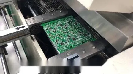
We specilized in : Ucreate is specialized in the production of a variety of single, double, high multi layers, HDI, the metallic substrate and FPC PCB. With laser drilling machine, CNC drilling machine, automatic machine, automatic exposure machine, large-scale lamination machine, Automatic flow production line, auto panel plating line, auto P.T.H Line, and other precision production equipments and AOI testing machine, flying probe tester machine and other advanced detection equipments.Production processes:Material Receiving → IQC → Stock → Material to SMT → SMT Line Loading → Solder Paste/Glue Printing → Chip Mount → Reflow → 100% Visual Inspection → Automated Optical Inspection (AOI) → SMT QC Sampling → SMT Stock → Material to PTH → PTH Line Loading → Plated Through Hole → Wave Soldering → Touch Up → 100% Visual Inspection → PTH QC Sampling → In-Circuit Test (ICT) → Final Assembly → Functional Test (FCT) → Packing → OQC Sampling → ShippingPCB assembly Equipment:1. High speed and precision chip placer or multi-function SMD mounter2. Wave soldering machine3. Vacuum machine4. High temperature box5. Auto-solder paste printer6. Hot- and mixed-air reflow
Required informations:1. Components list(a) Specification, brand, footprint(b)To short the lead time, please kindly advise us if there is any acceptable components substitution.(c) Schematic if necessary2. PCB board information(a) Gerber files(b) PCB board processing technic3. Testing Guide & Test Fixtures if necessary4. Programming files & Programming tool if necessary5. Package requirementWhy Choose Us?1. Your inquiry related to our products or prices will be replied in 24hrs.2. Well-trained and experienced staffs to answer all your enquires in fluent English3. OEM&ODM, we can help you to design and put into product.4. Distributorship are offered for your unique design and some our current models5. Protection of your sales area, ideas of design and all your private informationTrade Terms:1. Payment: T/T in advance (Western Union , payple is welcomed)2. Production lead time 100PCS: 5-7days, 500~1000PCS: 7-10days, above 1000PCS 15-20days.3. Sample can be delivered in 3days4. Shipping freight are quoted under your requests5. Shipping port: Shen zhen,Mainland China6. Discounts are offered based on order quantities7. MOQ: 1PCSPackage &Shipping Methods:1.Vacuum package with silica gel, Carton box with packing belt.2. By DHL, UPS, FedEx, TNT3. By EMS (Usually for Russia Clients)4. By sea for mass quantity according to customer's requirementCertificates:
Send to us