
 Home
Home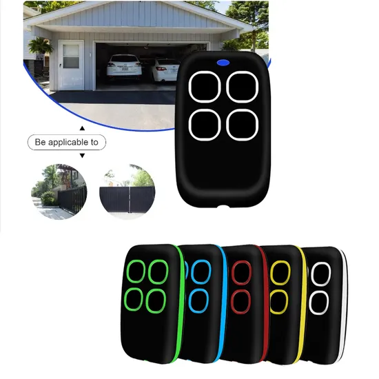

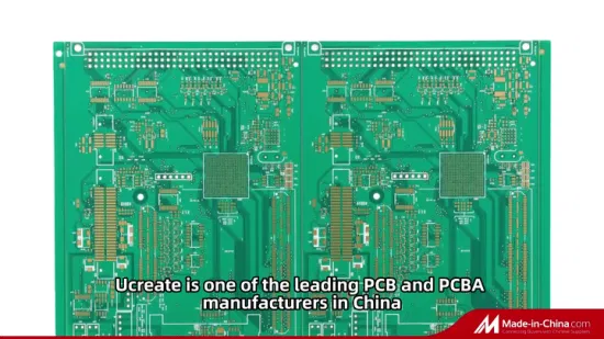
Ucreate Multilayer PCB Board Manufacturer in China Automotive Electronics PCBA HDI Board
Package Size 60.00cm * 50.00cm * 40.00cm Package Gross Weight 2.000kg Ucreate LTD PCB's aim: Customer Satisfaction is Al
Basic Info.
| Model NO. | UC-25412 |
| Application | Medical Instruments |
| Flame Retardant Properties | V0 |
| Mechanical Rigid | Rigid |
| Processing Technology | Electrolytic Foil |
| Base Material | Copper |
| Insulation Materials | Epoxy Resin |
| Brand | Uc |
| Ipc Standards | Ipc Class II |
| Base Material Type | Fr4 |
| Lead Time | 8 Working Days |
| Fast Turn | 3 Working Days |
| PCB Testing | E-Testing, Flying Probe Testing |
| Soldermask Color | Green |
| Specialities | Controlled Impedance |
| Surface Finish | Enig/3u′′ |
| Board Layer | 16 |
| Board Thickness | 3.2mm |
| Transport Package | Vacuum Pacakage |
| Specification | UL(US&Canada). ISO9001. RoHs, TS, SGS |
| Trademark | UC |
| Origin | Shenzhen, China |
| HS Code | 85340010 |
| Production Capacity | 20000sqm/Month |
Packaging & Delivery
Package Size 60.00cm * 50.00cm * 40.00cm Package Gross Weight 2.000kgProduct Description
Ucreate LTD PCB's aim:Customer Satisfaction is Always Our First Priority!
*Quality Policy *Top Quality and high efficiency *Improve continuously *Achieve customer's satisfaction
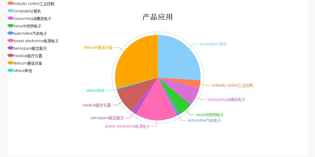
1.Products Application:
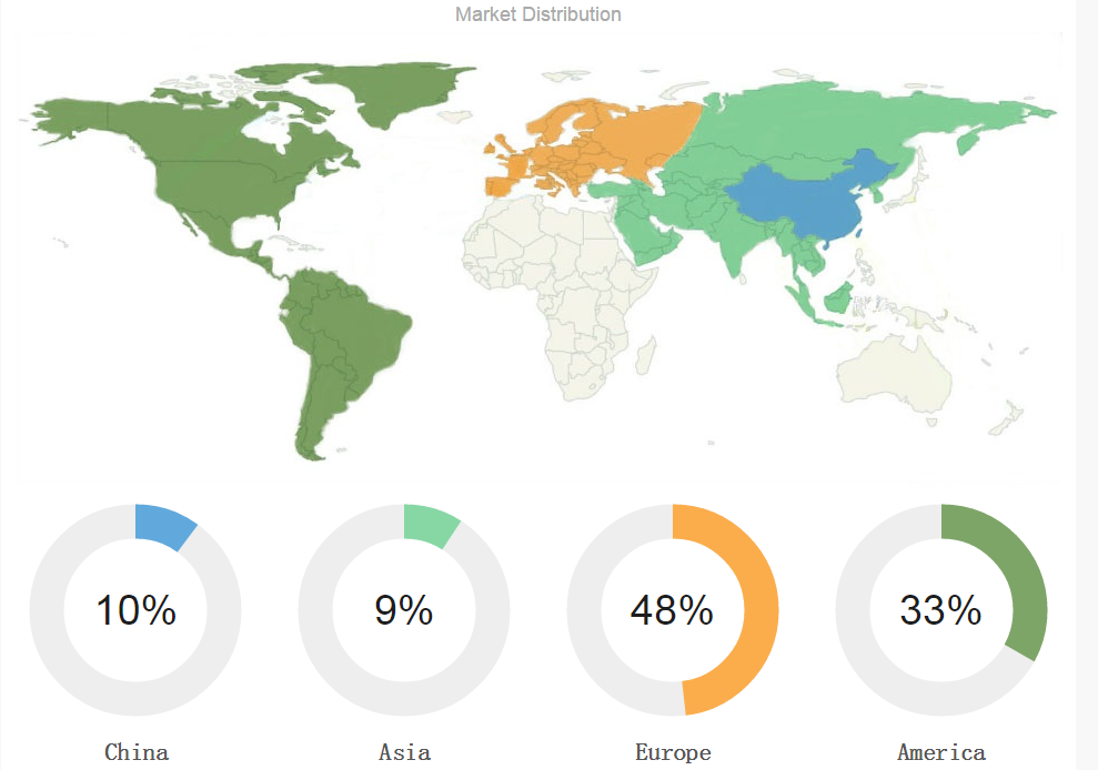
2. Market Distribution:
3.Technical Capabilities:
| Items | Speci. | Remark | |
| Max panel size | 32" x 20.5"(800mm x 520mm) | ||
| Min trace width/ space (inner layer) | 4mil/4mil(0.1mm/0.1mm) | ||
| Min PAD (inner layer) | 5 mil(0.13mm) | hole ring width | |
| Min thickness(inner layer) | 4 mil(0.1mm) | without copper | |
| Inner copper thickness | 1~4 oz | ||
| Outer copper thickness | 0.5~6 oz | ||
| Finished board thickness | 0.4-3.2 mm | ||
Board thickness tolerance control | ±0.10 mm | ±0.10 mm | 1~4 L |
| ±10% | ±10% | 6~8 L | |
| ±10% | ±10% | ≥10 L | |
| Inner layer treatment | brown oxidation | ||
| Layer count Capability | 1-30 LAYER | ||
| alignment between ML | ±2mil | ||
| Min drilling | 0.15 mm | ||
| Min finished hole | 0.1 mm | ||
| Hole precision | ±2 mil(±50 um) | ||
| tolerance for Slot | ±3 mil(±75 um) | ||
| tolerance for PTH | ±3 mil(±75um) | ||
| tolerance for NPTH | ±2mil(±50um) | ||
| Max Aspect Ratio for PTH | 8:1 | ||
| Hole wall copper thickness | 15-50um | ||
| Alignment of outer layers | 4mil/4mil | ||
| Min trace width/space for outer layer | 4mil/4mil | ||
| Tolerance of Etching | +/-10% | ||
| Thickness of solder mask | on trace | 0.4-1.2mil(10-30um) | |
| at trace corner | ≥0.2mil(5um) | ||
| On base material | ≤+1.2mil Finished thickness | ||
| Hardness of solder mask | 6H | ||
| Alignment of solder mask film | ±2mil(+/-50um) | ||
| Min width of solder mask bridge | 4mil(100um) | ||
| Max hole with solder plug | 0.5mm | ||
| Surface finish | HAL (Lead or Lead free), immersion Gold, Immersion Nickel, Electric Gold finger, Electric Gold, OSP, Immersion Silver. | ||
| Max Nickel thickness for Gold finger | 280u"(7um) | ||
| Max gold thickness for Gold finger | 30u"(0.75um) | ||
| Nickel thickness in Immersion Gold | 120u"/240u"(3um/6um) | ||
| Gold thickness in Immersion Gold | 2u"/6u"(0.05um/0.15um) | ||
| Impedance control and its tolerance | 50±10%,75±10%,100±10% 110±10% | ||
| Trace Anti-stripped strength | ≥61B/in(≥107g/mm) | ||
| bow and twist | 0.75% | ||
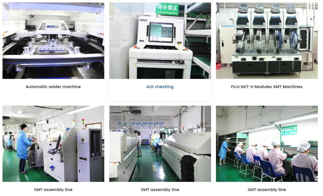
4.Products Equipment:
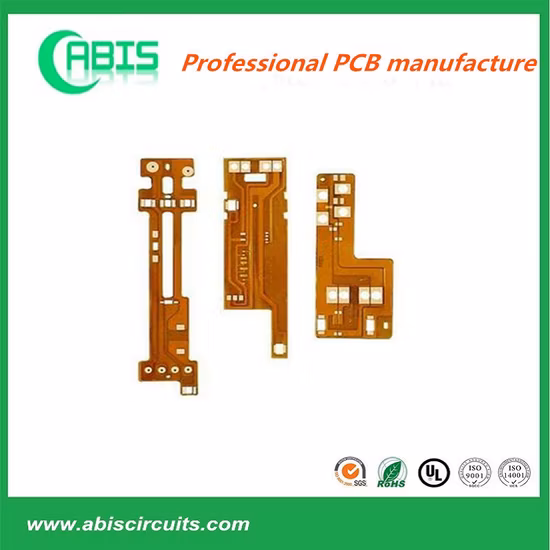
Product Description:
*Layers: 1-22
*Base material: FR-4 CEM-1
*Thickness: 0.2-5.0mm
*Solder mask: Green, black, red, yellow, white
*Min. Line width: 0.075mm
*Min. Line space: 0.075mm
*Min. Hole diameter: 0.1mm
*Surface treatment: Immersion gold, OSP. Lead free HASL.
*Blind/buried via holes: OK
*lead time: Seven to ten days (HDI: About 30 days)
We can also make quick pcb. As customers plates copied from the PCB, PCB design, prototype production, production, processing, and other SMT one-stop service.
Single-double sides pcb delivery time: 12-24 hours
4 layer- 8 layer pcb delivery time: 48-96 hours
We specilized in :
Ucreate is specialized in the production of a variety of single, double, high multi layers, HDI, the metallic substrate and FPC PCB. With laser drilling machine, CNC drilling machine, automatic machine, automatic exposure machine, large-scale lamination machine, Automatic flow production line, auto panel plating line, auto P.T.H Line, and other precision production equipments and AOI testing machine, flying probe tester machine and other advanced detection equipments.
Production processes:
Material Receiving → IQC → Stock → Material to SMT → SMT Line Loading → Solder Paste/Glue Printing → Chip Mount → Reflow → 100% Visual Inspection → Automated Optical Inspection (AOI) → SMT QC Sampling → SMT Stock → Material to PTH → PTH Line Loading → Plated Through Hole → Wave Soldering → Touch Up → 100% Visual Inspection → PTH QC Sampling → In-Circuit Test (ICT) → Final Assembly → Functional Test (FCT) → Packing → OQC Sampling → Shipping
PCB assembly Equipment:
1. High speed and precision chip placer or multi-function SMD mounter
2. Wave soldering machine
3. Vacuum machine
4. High temperature box
5. Auto-solder paste printer
6. Hot- and mixed-air reflow
Requested informations for PCBA:
1. Components list
(a) Specification, brand, footprint
(b)To short the lead time, please kindly advise us if there is any acceptable components substitution.
(c) Schematic if necessary
2. PCB board information
(a) Gerber files
(b) PCB board processing technic
3. Testing Guide & Test Fixtures if necessary4. Programming files & Programming tool if necessary5. Package requirement
Why Choose Us?
1. Your inquiry related to our products or prices will be replied in 24hrs.2. Well-trained and experienced staffs to answer all your enquires in fluent English3. OEM&ODM, we can help you to design and put into product.4. Distributorship are offered for your unique design and some our current models5. Protection of your sales area, ideas of design and all your private information
Trade Terms:
1. Payment: T/T in advance (Western Union , payple is welcomed)2. Production lead time 100PCS: 5-7days, 500~1000PCS: 7-10days, above 1000PCS 15-20days.3. Sample can be delivered in 3days4. Shipping freight are quoted under your requests5. Shipping port: Shen zhen,Mainland China6. Discounts are offered based on order quantities7. MOQ: 1PCS
Package &Shipping Methods:
1.Vacuum package with silica gel, Carton box with packing belt.2. By DHL, UPS, FedEx, TNT3. By EMS (Usually for Russia Clients)4. By sea for mass quantity according to customer's requirement
Certificates:

LED Copper Core PCB :next
Send to us