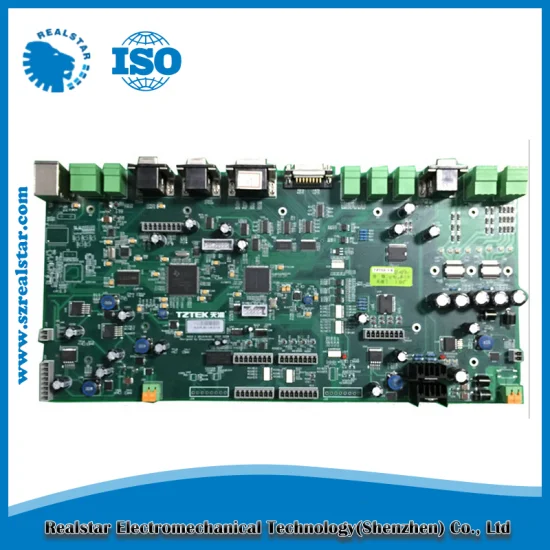
Diagnostic Medical Equipment PCB Assembly BGA PCBA with ISO13485 IATF16949
Basic Info.
| Condition | New |
| Trademark | YCD |
| Origin | Shenzhen China |
| HS Code | 8534001000 |
| Production Capacity | 5000PCS/Month |
Product Description
Product Description| Items | Capability |
| OEM PCB Layers | 1-28 layers |
| OEM PCB material | FR4, FR5, Aluminium,High Tg FR4, Halogen Free, Isola, Rogers |
| OEM PCB Finished Board Thickness | 0.2mm ~ 7.0mm(8mil-276mil) |
| OEM PCB Copper Thickness | 1/3oz ~ 7oz |
| OEM PCB Max gold plating thickness | 50 microinch |
| OEM PCB Min. Trace Width/Space | 0.075/0.075mm(3/3mil) |
| OEM PCB Min. Finish Holes Size | 0.1mm(4mil) for laser holes; 0.2mm(8mil) for mechanical holes |
| OEM PCB Max.Finshed Size | 600mm x 900mm (23.6" x 35.43" |
| OEM PCB Hole Tolerance | PTH:±0.076mm(+/-3mil), NTPH:±0.05mm(+/-2mil) |
| OEM PCB Soldermask Color | Green, White, Black, Red, Yellow, Blue,ect |
| OEM PCB Silkscreen Color | White, Black, Yellow, Blue |
| OEM PCB Impedance Control | +/-10% |
| OEM PCB Profiling Punching | Routing, V-CUT, Chamfer |
| OEM PCB Special Holes | Blind/Buried holes, Countersunk holes |
| OEM PCB Surface Finishing | HASL, Lead Free HASL, Immersion tin, Immersion gold, Gold plating, Immersion silver, OSP, Carbon, etc. |
| OEM PCB Certificate | UL, ISO9001, ROHS, SG |
Company Profile
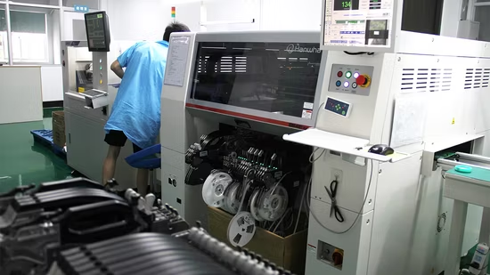
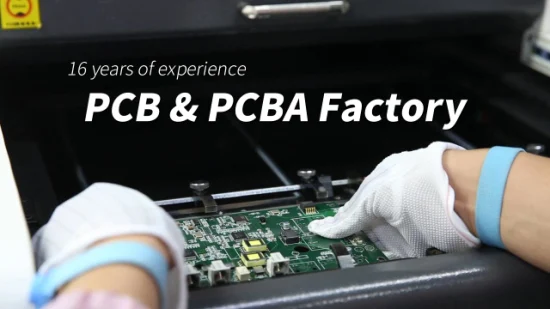
We have more than 10 years of SMT manufacturing experience, well appointed SMT ,DIP and assembly lines, offering one stop service from SMT,FPC,DIP,EMS, conformal coating, testing, final assembly, component procurement ,design, peripheral products support and so on. we are equipped with High-speed and accurately SMT Equipment ,and we provide a whole range of SPI,AOI,ICT,FCT,X-RAY,ROHS and aging testing for products. All ourshop floors are dust free, all lines are lead free, we are ISO9001 certified company.
Equipment
Production
DIP Multiplayer PCBA
1. What files do you use in PCB and assembly Quotation? Gerber, pcb. Auto CAD + Bill of Material2. How do you make sure the quality? Our Product is all 100% tested including Flying Probe Test (for sample), E-test (mass) or AOI.3. Can we visit your company? Of course! Welcome to visit our company, Grandtop is located in Hualun Tech Park, Shenzhen, Guandong province, china.4. What is the lead time? It takes 3-5 working days for sample, 7-10 working days for batch production based on files and quantity.5. Will you keep our information and files secret? Sure! It is our basic principle to keep business secrets to protect our customers' rights and behalf.6. How to work with you? -Email and send us the PCB layout file, BOM list - We will provide reply confirmation within 12 hours and reply to the offer within 3-5 days. - Waiting for your company to confirm the price, order and payment method. - We will start the production.


